Oscilloscope Tracings
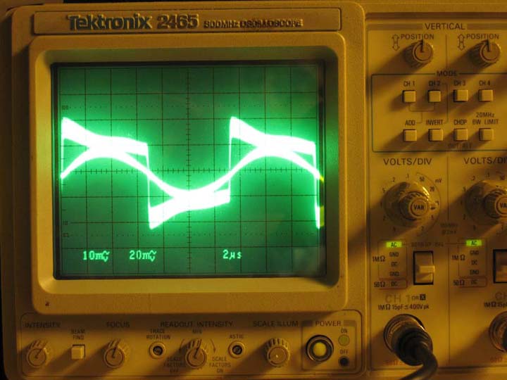
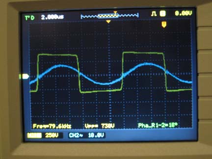
Now, if the tanks is above resonance we have more inductive reactance. The tank's net current will lag the driving voltage from the coupling transformer. Since the input and output current of the coupling transformer are in phase, the tank's current is lagging the inverter driving voltage. Below you can see the dominating inductive reactance results in the inverter current (triangle-looking wave) is almost 90 degrees lagging the inverter voltage (square wave).
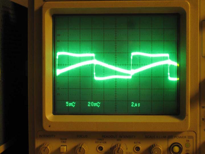
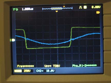
If we are below the resonant frequency capacitive reactance results in the current leading the inverter voltage. Also, there is ringing in the current waveform and at the inverter voltage transitions. This noise gets worse with higher power levels and can result in mosfet failure.
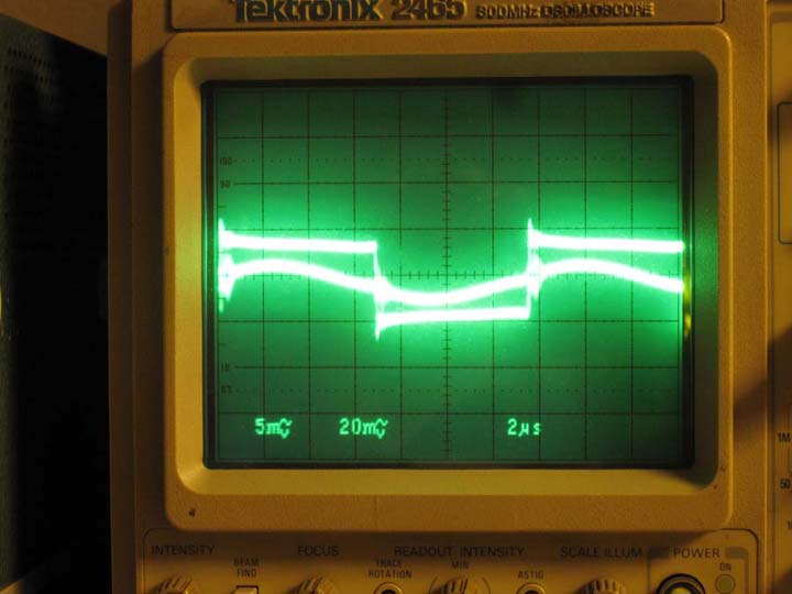
Below is another example of ringing. You can see ringing on the voltage at the transition and on the current waveform. I have positioned them apart for easier viewing. This is due to high inductance on the gate. Heavy current on the gate causes a large Ldi/dt. The problem can usually be solved by either increasing the gate resistance (increase the resistor value), or decrease the stray inductance by shortening the gate lead. I was able to almost eliminate the ringing by shortening the gate lead, but then I did not have enough length for connecting two in parallel. So I changed the value of R from 5 ohms to 10 ohms. The first image is with the 5 ohm gate resistor. I was still able to charge the gate with 10 ohms in a sufficiently short amount of time at 15v.
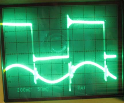
These images show the waveform after the fix: shortening the gate leads as much as possible to still allow room for paralleling two of them and increasing the gate resistor from 5R to 10R. Notice the clean voltage square wave and the smooth current curve. The second image is a blow-up of the first.
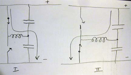
Below is a basic sketch of the half-bridge inverter. The coil in the middle is the coupling transformer to the resonant tank. The arrows show the paths the current takes as the switches alternate between closed-open and open-closed.
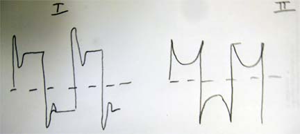
Below are two sketches. Sketch I shows ringing if there is too long of a delay during switching. If the next switch does not close in time, the inductive kick will drive the voltage too high, causing an overshoot, followed by a large dip when it finally closes. Sketch II shows profound voltage sagging in the middle of the waveform. I had this happen when the decoupling capacitors went bad, shorting the current path. The capacitors are needed to remove any DC component from the pulse.
I would like just mention that the inductive waveforms is really an exponential curve. If we can approximate the tank above resonane as a RL circuit responding to a step response
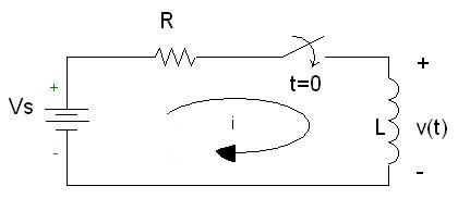
The solution to
is

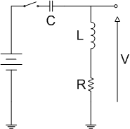
Analysis of a capacitor dominant RC circuit will yield something similar. When dealing with a RCL step response one has
![]()
and the 2nd order differential equation is
![]()
and the general solution is
![]()
If the system is underdamped the solution has the form:
V(t) = e-αt(Bcos(ѡt) + Bsin(ѡt))